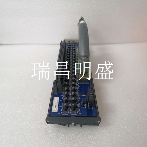
ICS T8830 工控機器人備件
DIP開關設置表20和表21描述了DIP開關陣列S1和S2的設置。對這些設置所做的更改僅在電源循環后生效。功能描述-CAN型號圖8-帶引腳位置的CAN板,示教按鈕表22顯示了用于CAN控制器型號的主連接器J2上的引腳分配。該擴展PCB配有兩個RJ45連接器J12和J13,用于CAN接口。表23描述了引腳功能。表19-RS-485控制器狀態指示燈狀態指示燈描述顏色含義D8數據通信關閉無通信綠色閃爍通信激活D9 RS-485錯誤關閉無RS-485錯誤紅色RS-485錯誤表20-主PCB功能DIP開關陣列S1上的DIP開關設置(0:Off,1:on,X:不相關)8765432 1默認值0 0 0 0偏移到地址:0(00 Hex)X X X 0 0 0 0地址偏移:1(01 Hex)X X X 0 1 0 1地址偏移:2(02 Hex)XX X 0 10 1 0地址偏移量:3(03 Hex)X-X X 0 01 1 1地址偏移量4(04 Hex)X.X X 0 100 0地址偏移值:5(05 Hex)X/X 0 1 1 0 1偏移量:6(06 Hex)/X X 0 1 10地址偏移量7(07 Hex)2X 0 1 1 1偏移量8(08 Hex).X 1 0 0 0偏移量這是一個很好的例子到地址:9(09 Hex)X X X 1 0 0 1到地址的偏移:10(0A Hex)X X X 1 1 0 0到地址的偏置:11(0B Hex)XX X 10 1 1到地址:12(0C Hex)X-X X 1 10 0到地址:13(0D Hex)X X 1 11 0到地址偏移:14(0E Hex)X1 X 1 1 1 0到地址上的偏移:15(0F Hex)X2 1 1 1 1通信速率19200 Baud X 0 X X X X通信速率2400 Baud XX 0 1 X X X X通信速率9600 Baud X X 1 0 X X X X通信速率57600 Baud X 1 X X 1 X X X X重置為默認值1 X X X X X X表21-雙列直插式開關陣列S2 2線(默認)/4線通信設置(在擴展PCB上)功能雙列直插開關陣列S2 4321默認值0 1 0端接電阻器(135 W)OFF X X 0端接電阻(135W)on X X 1端接電阻器4線OFF X X 0 0終端電阻器4線ON X X 1 1 Rx 2線0 1 0 X Rx 4線1 0 X X表22-J2引腳列表引腳信號說明備注1 0V DC電源-2+24V DC電源-3接地-4未連接未連接-5輸入2觸發和保持參見出版物10000071139 6輸入1未使用未使用7輸出2燈陣列中斷(1)(1)或超高(特殊功能)0V DC=中斷24V DC=未中斷8輸出1懸垂0V DC=懸垂24V DC=無懸垂表23-J12和J13引腳信號的CAN標準RJ45連接
DIP Switch Settings Table 20 and Table 21 describe settings for DIP switch arrays S1 and S2. Changes made to these settings take effect only after a power cycle. Functional Description — CAN Model Figure 8 - CAN Board with Pin Locations, Teach Button Table 22 shows the allocation of pins on the main connector, J2, for use with the CAN controller model. This extension PCB is equipped with two RJ45 connectors, J12 and J13, for the CAN interface. Table 23 describes pin functions. Table 19 - RS-485 Controller Status Indicators Status Indicator Description Color Meaning D8 Data communication Off No communication Green flashing Communication active D9 RS-485 Error Off No RS-485 error Red RS-485 error Table 20 - DIP Switch Array S1 Settings on the Main PCB Function DIP switch array S1 (0: OFF, 1: ON, X: not relevant) 8765432 1 Default 0 0 0 0 0 0 0 0 Offset to address: 0 (00 Hex) X X X X 0 0 0 0 Offset to address: 1 (01 Hex) X X X X 0 0 0 1 Offset to address: 2 (02 Hex) X X X X 0 0 1 0 Offset to address: 3 (03 Hex) X X X X 0 0 1 1 Offset to address: 4 (04 Hex) X X X X 0 1 0 0 Offset to address: 5 (05 Hex) X X X X 0 1 0 1 Offset to address: 6 (06 Hex) X X X X 0 1 1 0 Offset to address: 7 (07 Hex) X X X X 0 1 1 1 Offset to address: 8 (08 Hex) X X X X 1 0 0 0 Offset to address: 9 (09 Hex) X X X X 1 0 0 1 Offset to address: 10 (0A Hex) X X X X 1 0 1 0 Offset to address: 11 (0B Hex) X X X X 1 0 1 1 Offset to address: 12 (0C Hex) X X X X 1 1 0 0 Offset to address: 13 (0D Hex) X X X X 1 1 0 1 Offset to address: 14 (0E Hex) X X X X 1 1 1 0 Offset to address: 15 (0F Hex) X X X X 1 1 1 1 Communication rate 19,200 Baud X X 0 0 X X X X Communication rate 2400 Baud X X 0 1 X X X X Communication rate 9600 Baud X X 1 0 X X X X Communication rate 57,600 Baud X X 1 1 X X X X Reset to default 1 X X X X X X X Table 21 - DIP Switch Array S2 Settings for 2-Wire (default)/4-Wire Communication (on extension PCB) Function DIP switch array S2 4321 Default 0 1 0 0 Terminating resistor (135 W) OFF X X X 0 Terminating resistor (135 W) ON X X X 1 Terminating resistor 4-wire OFF X X 0 0 Terminating resistor 4-wire ON X X 1 1 Rx 2-wire 0 1 0 X Rx 4-wire 1 0 X X Table 22 - J2 Pin Listings Pin Signal Description Remarks 1 0V DC Power — 2 +24V DC Power — 3 Ground Ground — 4 Not connected Not connected — 5 In 2 Trigger and hold See Publication 10000071139 6 In 1 Not used Not used 7 Out 2 Light array interrupted (1) (1) Or over-height (special function) 0V DC = interrupted 24V DC = not interrupted 8 Out 1 Overhang 0V DC = overhang 24V DC = no overhang Table 23 - CAN Standard RJ45 Connection for J12 and J13 Pin Signal


