


產品詳情介紹
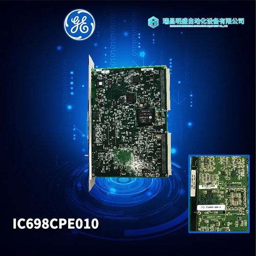
IS215ACLEH1A燃機模塊
當其中一個輸入相位脫落時Q108的傳導周期縮短,電容器C129開始充電。在三個線路頻率周期后,C129充電充足,導致Q109傳導,從而有效地使驅動電路接地,防止產生進一步的SCR門脈沖,從而關閉裝置的輸出。當交流輸入降到工作范圍以下時,交流斷開電路可防止電源工作。該電路的工作原理如下:C128將通過R149開始放電。這將導致Q107開始將點火線接地至SCR,并重置“軟啟動”電路。一旦輸入功率達到工作水平,“軟啟動”電路將按以下方式復位:電容器C134通過Q110的基極緩慢開始充電。隨著C134充電,基極電流將減小,從而使Q110的集電極電壓緩慢上升,從而逐漸增加SCR的導通角。為電壓和電流通道提供單獨的恒流參考。Q111的集電極電流驅動電壓通道,Q112驅動電流通道。這些電流源由溫度補償齊納二極管CR133兩端的電壓參考。由于IC104引腳1和2的求和結上的電壓差基本上為零,CR133上的電壓也出現在R167和R168的串聯組合上(由于Q111和Q112的Vbe基本上是恒定電流,所以R171和R173也是如此)。通過固定電阻的恒定電壓產生恒定的集電極電流。R167和R171可將每個電源的電流調節為1 mA。
電壓通道流的參考電流水平從J107-2到TB3-3。
端子TB3-3、4和5之間有跳線,當電流流過電壓控制R13時產生的電壓電平被施加到IC104的引腳8。IC104引腳9的其他輸入上的信號來自通過分壓器R177加上R178和R179的電源輸出電壓電平。IC104的針腳9處的最大額定輸出電壓產生+5Vdc。當R13處于完全順時針位置時,+5Vdc施加在IC104的引腳8上。如果衰減輸出電壓與R13設置的值不同(例如,由于負載變化),IC104引腳10的輸出端將產生錯誤信號。該錯誤信號通過SCR控制電路,將導致輸出電壓成比例變化,從而使IC104引腳9上的電壓等于施加在引腳8上的電壓。電流通道的作用與電壓通道的作用相同,但受控量通過分流器R12進行采樣除外。該采樣電壓與IC104引腳6上產生的參考電壓相比較,由前面板電流控制R14建立。(0至100毫伏直流電)。電壓通道放大器和電流通道放大器的輸出由二極管CR136和CR139“存儲”在一起。無論哪個通道具有較高的正輸出信號,都會覆蓋另一個通道的影響,成為控制直流輸出的通道。電壓或電流通道的輸出饋送至晶體管Q110的底座,晶體管Q110作為線性放大器工作,其輸出饋送到相位控制電路Q101-106。
When one of the input phases drops out
the conduction cycle of Q108 is reduced, allowing capacitor C129 to start charging. After three cycles of line frequency, C129 charges sufficiently to cause Q109 to conduct which effectively grounds the drive circuit preventing the generation of further SCR gate pulses which shuts down the output of the unit. The AC dropout circuit prevents the power supply from operating when the AC input drops below operating range. This circuit works as follows: C128 will start discharging through R149. This will cause Q107 to start conducting grounding the firing line to the SCRs and resets the "soft start" circuit. Once input power is at the operating level, the "soft start" circuit will reset in the following manner: Capacitor C134 slowly starts charging through the base of Q110. As C134 charges, the base current will decrease allowing the collector voltage of Q110 to slowly rise which gradually increases the conduction angle of the SCR's. Separate constant current references are provided for the voltage and current channels. The collector current of Q111 drives the voltage channel and Q112 the current channel. These current sources are referenced by the voltage across CR133, a temperature-compensated zener diode. Since the voltage difference across the summing junction of IC104 pins 1 and 2 is essentially zero, the voltage across CR133 also appears across the series combination of R167 and R168 (also R171 and R173 since the Vbe of Q111 and Q112 is essentially constant current). A constant voltage across a fixed resistance produces a constant collector current. The current from each of these sources is adjustable to 1 mA by R167 and R171.
The reference current level for the voltage channel flows
from J107-2 to TB3-3. With jumpers between terminals TB3-3, 4 and 5, the voltage level produced when this current flows through the VOLTAGE control R13 is applied to pin 8 of IC104. The signal on the other input of IC104 pin 9 is derived from the power supply output voltage level through voltage divider R177 plus R178 and R179. Maximum rated output voltage produces +5Vdc at pin 9 of IC104. With R13 in the fully clockwise position, +5Vdc is applied to pin 8 of IC104. If attenuated output voltage changes from the value set by R13 (because of load changes, for example) an error signal will be developed at the output of IC104, pin 10. This error signal, via the SCR control circuitry, will cause a proportional change in the output voltage so as to bring the voltage on pin 9 of IC104 equal to that applied to pin 8. The action of the current channel is identical to that of the voltage channel with the exception that the controlled quantity is being sampled across the shunt R12. This sampled voltage is compared to the reference voltage produced at pin 6 of IC104, which is established from the front panel current control R14. (0 to 100 millivolts DC).The output of the voltage channel amplifier and the current channel amplifier are "ored" together by diodes CR136 and CR139. Whichever channel has a higher positive output signal overrides the effect of the other and becomes the channel controlling the DC output. The output of either the voltage or current channel is fed to the base of transistor Q110 which operates as a linear amplifier whose output is fed to the phase control circuit Q101-106.
產品優勢
1:國外專業的供貨渠道,具有價格優勢
2:產品質量保證,讓您售后無憂
3:全國快遞包郵
4:一對一服務
公司主營范圍簡介
PLC可編程控制器模塊,DCS卡件,ESD系統卡件,振動監測系統卡件,汽輪機控制系統模塊,燃氣發電機備件等,優勢品牌:Allen Bradley、BentlyNevada、ABB、Emerson Ovation、Honeywell DCS、Rockwell ICS Triplex、FOXBORO、Schneider PLC、GE Fanuc、Motorola、HIMA、TRICONEX、Prosoft等各種進口工業零部件、歐美進口模塊。
產品廣泛應用于冶金、石油天然氣、玻璃制造業、鋁業、石油化工、煤礦、造紙印刷、紡織印染、機械、電子制造、汽車制造、塑膠機械、電力、水利、水處理/環保、鍋爐供暖、能源、輸配電等等
")