


")
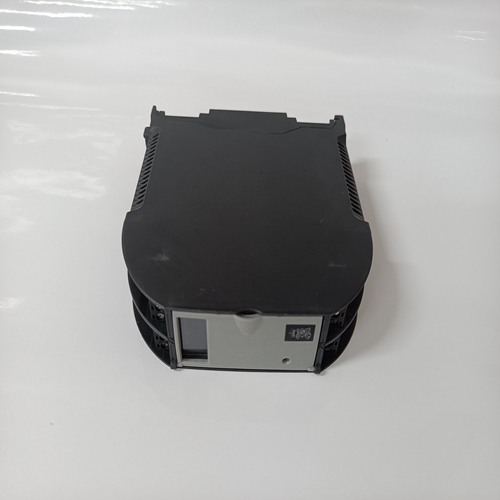
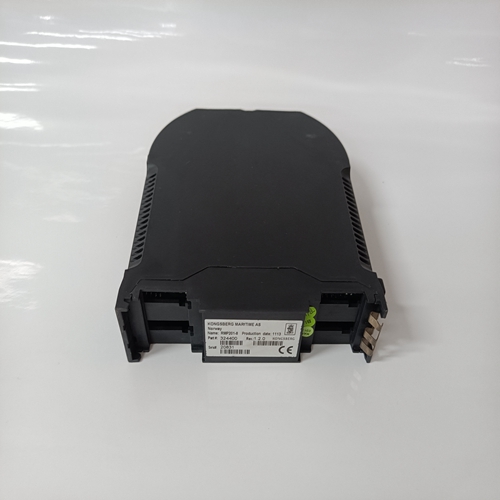
RMP201-8遠程控制器
每個發電機系統中連接的單元/并聯開關消除了關閉的發電機組中CT的串聯電阻正在運行的發電機組的CT。
錯誤檢測器:錯誤檢測器電路由電壓調節器組成電路、分壓器、兩級差分放大器? 呃,還有
內部次要反饋? 阿爾特。電壓調整電路包括:外部電壓調節變阻器VAR、電壓范圍調節R2和
? xed電阻器R1。外部電壓調整的全行程提供±10%
發電機輸出電壓從標稱值調整。電壓范圍調整R2確定最大和/或最小電壓
調整無功限制。電壓調整電路和分壓器由電阻器R5和R71組成,確定? rst微分放大器? 呃。
這個? rst差分級包括晶體管Q1、Q2和Q12,電阻器R9至R18、R21、R22、R23、R83和R93、電容器C3、C23、C30和C31、鐵氧體磁珠L2和L3、齊納二極管Z1和欠頻限制內的電路。低頻限值(UFL)
如上所述,向晶體管Q2的基極提供參考電壓
在UFL電路描述中。發電機額定運行期間頻率:參考信號是恒定的,與齊納相同
電壓來自感測電路的電壓,與發電機電壓施加到晶體管Q1的基極。當Q1基極
電壓不同于施加到基極的參考電壓Q2,Q1集電極電流相對于Q2將存在差異集電極電流。
來自晶體管Q1集電極的電流由電阻器分壓R9和R16
注入第二級差速器的底座
放大? 類似地,來自晶體管Q2集電極的電流被電阻器R14和R15分壓并注入第二級差分放大器? er晶體管Q4、電阻器R10和C3有助于防止高頻振蕩。第二階段微分放大器? er振幅? es是? 一級差動放大? 呃。第二級差速器中包含的部件放大? er是晶體管Q3和Q4以及電阻器R24至R27
晶體管Q3的集電極電壓控制相位控制電路。這個次要反饋? 濾波器由電阻器R8和電容器C2組成? 過濾器
從dc信號中去除任何剩余的ac。相位控制電路:T1的一個次級繞組、二極管D1、D2,D21和D22、電阻器R87和R88、電容器C20、C21和C22、電源權力? rst和第二差分級以及欠頻
極限階段。相位控制電路由二極管D5和D6組成,電阻器R28至R32和R80、電容器C20、C21和C22、齊納二極管Z2和可編程單結晶體管(PUT)Q5。
相位控制電路是斜坡和基座控制,用于調節:功率控制器電路的相位角通過控制
它向SCR的柵極提供接通信號。指數斜坡從電壓基座開始的電壓提供開啟選通
信號因為斜坡電壓從電壓基座開始基座電壓振幅的小變化導致大SCR相位角的變化如圖2所示。
A unit/parallel switch connected in each generator system eliminates the
series resistance of the CTs in the generator sets that are shut down from
the CTs of the generator sets that are operating.
Error detector: The error detector circuitry consists of a voltage adjust
circuit, a voltage divider, a two-stage differential ampli? er, and an
internal minor feedback ? lter. The voltage adjust circuit consists of an
external voltage adjust rheostat VAR, a voltage range adjustment R2, and
? xed resistor R1. Full travel of the external voltage adjust provides ±10%
adjustment of the generator output voltage from nominal. The voltage
range adjustment R2 establishes the maximum and/or minimum voltage
adjust limit of VAR. The voltage adjust circuit and a voltage divider
consisting of resistors R5 and R71 determine the input signal to the ? rst
differential ampli? er.
The ? rst differential stage is comprised of transistors Q1, Q2, & Q12,
resistors R9 through R18, R21, R22, R23, R83, & R93, capacitors
C3, C23, C30, & C31, ferrite beads L2 & L3, Zener diode Z1, and the
circuitry within the underfrequency limit. Underfrequency limit (UFL)
provides a reference voltage to the base of transistor Q2 as described
in the UFL circuit description. During generator operation at rated
frequency the reference signal is constant and identical to the Zener
voltage. Voltage from the sensing circuit, which is proportional to the
generator voltage, is applied to the base of transistor Q1. When Q1 base
voltage is different from the reference voltage applied to the base of
Q2, there will be a difference in Q1 collector current with respect to Q2
collector current.
The current from the collector of transistor Q1 is divided by resistors
R9 and R16 and injected into the base of the second stage differential
ampli? er transistor Q3. Similarly, the current from the collector of transistor Q2 is divided by resistors R14 and R15 and injected into the
second stage differential ampli? er transistor Q4. Resistors R10 and
C3 help to prevent oscillations at high frequencies. The second stage
differential ampli? er ampli? es the output of the ? rst stage differential
ampli? er. Components included in the second stage differential
ampli? er are transistors Q3 and Q4, and resistors R24 through R27. The
collector voltage of transistor Q3 controls the phase control circuit. The
minor feedback ? lter consists of resistor R8 and capacitor C2. The ? lter
removes any remaining ac from the dc signal.Phase control circuit: One of T1?s secondary windings, diodes D1, D2,
D21 & D22, resistors R87 & R88, capacitors C20, C21, & C22, supply
power to the ? rst and second differential stage and the underfrequency
limit stage. The phase control circuit consists of diodes D5 and D6,
resistors R28 through R32, & R80, capacitors C20, C21, & C22, Zener
diode Z2, and programmable unijunction transistor (PUT) Q5.
The phase control circuit is a ramp-and-pedestal control that regulates
the phase angle of the power controller circuit SCRs by controlling the
turn on signal it supplies to the gate of the SCRs. An exponential ramp
voltage that starts from a voltage pedestal provides the turn on gating
signal. Because the ramp voltage starts from the voltage pedestal, a
small change in the amplitude of the pedestal voltage results in a large
change in SCR phase angle as shown in Figure 2.