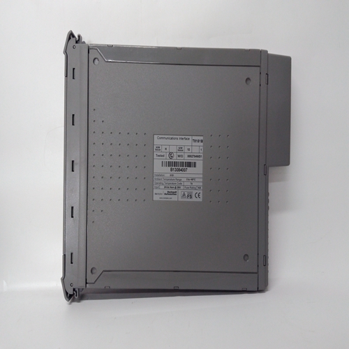
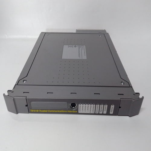
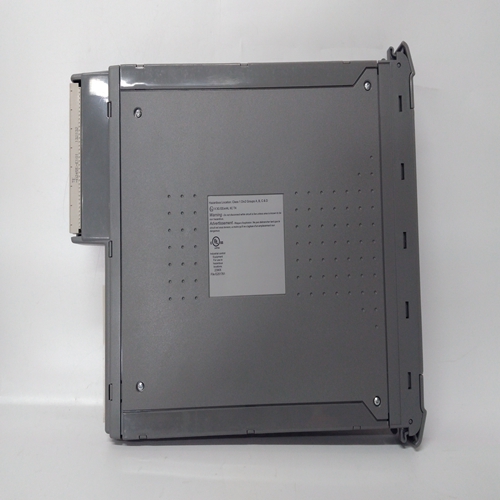
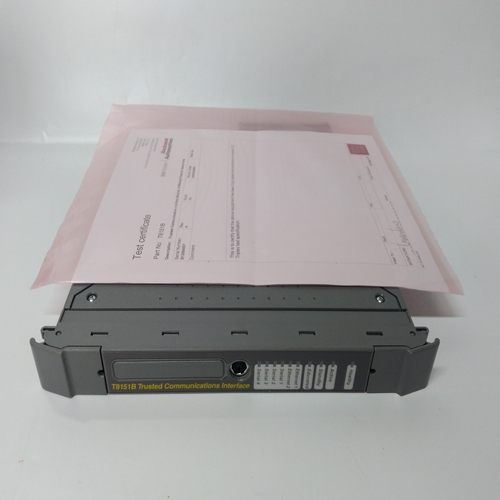
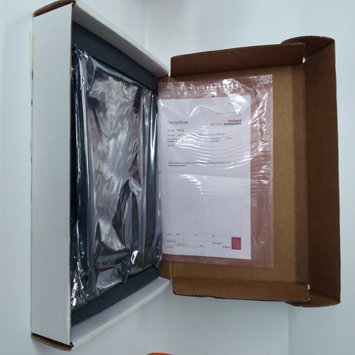
ICS TRIPLEX T8161B處理器模塊
LL_功能塊提供超前和滯后功能。只有通過設置TLEAD,塊才能用作滯后時間為0.0。滯后功能始終處于活動狀態,并具有最小設置為0.01分鐘。輸入E斷言高(1)將啟用超前/滯后作用當斷言為低(0)時,超前/滯后功能將被旁路,輸出將設置為等于輸入如果未配置輸入E,則塊將為啟用。LMT_功能塊用于限制實際信號。輸入A通常會通過功能塊,以:輸出O1。如果輸入超過其中一個限制,則塊將輸出極限值。如果HI限值設置為低于LO限值,則塊將輸出高限值。輸出狀態將:當塊處于極限狀態時,為高(1)。固件1.30及更高版本中的LN_功能塊將輸出輸入X的自然對數。當輸入<=0.0時,輸入將被視為大于0.0的最小數字(即1.17…e-38),以及將相應地計算LN。固件1.30及更高版本中的LOG__功能塊將輸出輸入X的底10的對數。當輸入<=0.0時,輸入將被視為大于0.0的最小數字(即1.17…e-38),并且將根據第m個功能塊計算日志。功能塊提供通用算術能力。如方框圖所示,每個輸入具有增益和偏置縮放。然后應用生成的信號到可配置的數學運算(DIV、MUL、ADD和SUB)。
操作A將首先在輸入A和上執行B、 接下來將對結果和執行操作B輸入C。
MUL或DIV操作的未使用輸入將設置為1.0而加法或子運算的值將設置為等于0.0.這些輸入的操作將正常運行因此,確保偏置和增益設置為:設置正確。
在DIV操作中,當除數為0.0時,輸出將繼續最大實數,符號由分子。如果分子為0,輸出將為0。MUL_功能塊對三個輸入信號。任何未使用的輸入都將設置為1.0因此對輸出沒有影響。NND_功能塊在三個輸入。任何未使用的輸入將設置為高(1)。NOR_功能塊對三個執行邏輯NOR輸入。任何未使用的輸入都將設置為低(0)。NOT_功能塊對輸入執行邏輯NOTA、 任何未使用的輸入都將設置為低(0)。
LL_ function blocks provide both lead and lag functions.
The block can function as lag only by setting the TLEAD
time to 0.0. The lag function is always active and has a
minimum setting of 0.01 minutes.
Input E asserted high (1) will enable the Lead/Lag
function. When asserted low (0), the Lead/Lag function
will be bypassed and the output will be set equal to the
input. If input E is not configured, the block will be
enabled. LMT_ function blocks are used to limit a real signal.
Input A will normally pass through the function block to
the output O1. If the input exceeds one of the limits, the
block will output the limit value.
If the HI LIMIT is set lower than the LO LIMIT, the block
will output the high limit value. The output statuses will
be high (1) when the block is in a limit condition. LN_ function blocks, in firmware 1.30 and higher, will output the
natural logarithm of input X. When the input is <= 0.0, the input will
be treated as the smallest number greater than 0.0 (i.e. 1.17....e-38) and
the LN will be computed accordingly. LOG__ function blocks, in firmware 1.30 and higher, will output
the logarithm to the base 10 of input X. When the input is <= 0.0,
the input will be treated as the smallest number greater than 0.0
(i.e. 1.17....e-38) and the LOG will be computed according MTH_ function blocks provide universal arithmetic
capability. As shown in the block diagram, each input has
gain and bias scaling. The resulting signals are then applied
to configurable math operations (DIV, MUL, ADD and
SUB). Operation A will be performed first on inputs A and
B. Operation B will be performed next on the resultant and
input C.
Unused inputs to a MUL or DIV operation will be set to 1.0
and those to an ADD or SUB operation will be set equal to
0.0. The operation of those inputs will function normally
so it is important to insure that the bias and gain settings are
set properly.
In a DIV operation, when a divisor is 0.0 the output will go
to the maximum Real number with the sign determined by
the numerator. If the numerator is 0 the output will be 0. MUL_ function blocks perform arithmetic multiplication on
the three input signals. Any unused input will be set to 1.0
and will therefore have no affect on the output. NND_ function blocks perform a logical NAND on the
three inputs. Any unused input will be set high (1). NOR_ function blocks perform a logical NOR on the three
inputs. Any unused input will be set low (0). NOT_ function blocks perform a logical NOT on input
A. Any unused input will be set low (0).


